


What Is Digital Logic NOT Gate (Inverter)? Its Symbols, Schematic Designs & IC Details
Table of Contents
What Is Logic NOT Gate (Inverter)?
A Digital logic gate which produces logic True when its input is False & generates logic False when its input is True is known as NOT gate or oftenly known as Inverter.

Basically, NOT gate is an Inverter. It inverts its input logic into the output. It implements the logical inversion function. NOT gate is a single input single output gate.
Symbol
There are three different symbols used for NOT gate:
ANSI
The American National standard Institute symbol, it is most commonly used:

IEC
The International Electrotechnical Commission symbol:

DIN
Deutsches Institut für Normung symbol for NOT gate, which is used in Germany:

Truth Table
The truth table is a logic table containing the input combinations and their corresponding outputs.
Assume a NOT gate with the input I & output O.
The truth table of NOT gate is given below:
| Input | Output |
| 0 | 1 |
| 1 | 0 |
It shows when the input is ‘1‘ or True, its output in ‘0‘ or False. And when the input is ‘0‘ or False, its output is ‘1‘ or True.
Expression
The expression for NOT gate uses the symbol ‘!‘ or ‘~‘ as shown in the expression below:
O = !I or O = ~I
Schematic Design
NOT gate cannot be designed using diodes, because diodes do not have inversion property and they cannot invert an input signal. However, Transistor can invert any signal. So we will discuss schematic designs using different transistors.
Resistor-Transistor Logic
RTL (Resistor-Transistor Logic) logic uses resistors and transistors to implement any logic function. Bi-polar junction transistors (BJT) are mainly of two types i.e. NPN & PNP. We will discuss the schematic designs using both of them separately in this article.
Using NPN
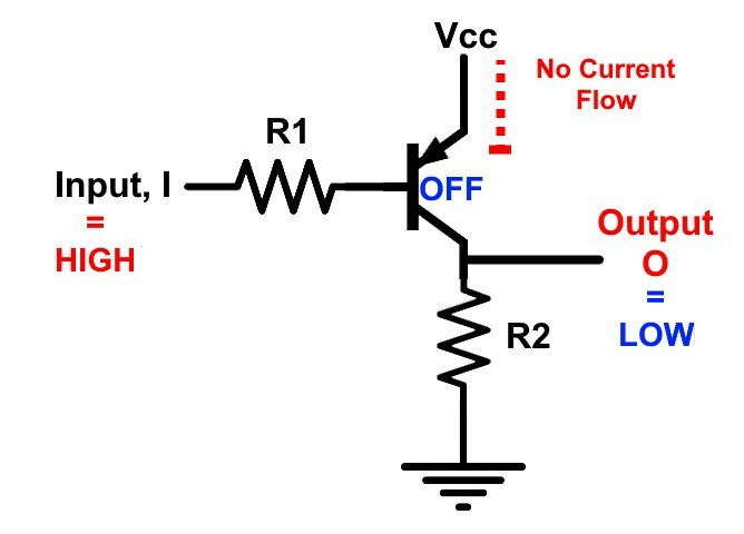
The schematic design of NOT gate using NPN transistors is:

Explanation:
In this schematic design, the collector of NPN is connected with resistor R2, which is connected with Vcc. The emitter of NPN is connected directly to the GND.
The output is taken from the collector terminal of NPN. The input line is connected to the base of the transistor through a resistor R1.
The supply voltage Vcc = 5v is applied to the circuit. Input True logic is 5v and False logic is 0v.
We will discuss this schematic for both cases of input logic
Case 1:
When the input is logic Low i.e. False or 0, the NPN transistor will switch off because there is no base current. As a result, there is no current flow through the transistor. So a conductive path will be established between Vcc and output, which makes the output logic High.

Case 2:
In this case, the input logic is High 5v i.e. True or 1, the NPN transistor will switch on & a conductive path from the output to ground is created. This path results in the output as logic Low.

Using PNP:
The schematic design of NOT gate using PNP transistor is given below:

Explanation:
In this design, the collector is connected with Vcc of 5v & the emitter is connected to the resistor R2 which is grounded.
The output O is taken across the resistor R2 & input is applied to the base of the transistor through resistor R1.
We will discuss this design for both cases of input logic.
Case 1:
When the input is logic High, the PNP transistor will switch off because its base input is logic High. As a result, there will be no current flow because of the breaking of the current flow path.
The output becomes connected to the ground, which is logic low as output.
Case 2:
When the input is logic Low, the PNP transistor will switch on because its base input is Low. Thus the path for the flow of current will complete & there will be voltage developed across resistor R2.
This voltage across resistor R2 is taken as the output, which is logic High.

MOS Logic
MOS logic uses Mosfets as the switching devices to implement any logic function. Mosfets such as NMOS, PMOS & CMOS are used in these designs. Mosfets are more economical because of their small sizes & low power consumption. It operates on input voltages. on the contrary, BJT operates on input current.
NMOS Design
The schematic design of NOT gate using NMOS transistor is given below:

This NOT gate design using NMOS shows that its drain is connected to a resistor R, which is connected to supply voltage Vdd. The Source of NMOS is connected to ground.
Input is directly applied to its gate, it does not need input resistor because it operates on input voltage rather than the input current.
The output is taken between the resistor R & the drain of the NMOS.
Operation:
When input logic is high, the NMOS switches on & the current path from Vdd to GND is complete. The output O is directly connected to GND, which is logic Low.

When the input is logic Low, the NMOS switch off & the current flow path breaks. Thus the supply voltage Vdd is routed as output O, which is logic High.

PMOS Design:
The design schematic of NOT gate using PMOS is given below:

In this design, the Drain of PMOS is directly connected to the supply voltage Vdd & the source is connected to resistor R, which is connected to GND.
Input is applied through the gate & the output is taken between the source & resistor R.
Operation:
When the input is logic high, the PMOS will switch off & there will be no flow of current because of the breaking of the conductive path. As a result, the output will connect with GND, which is logic low.

When the input is logic Low, the PMOS will switch on. Resulting in the creating a path for the flow of current. this current flow develops a potential across the resistor R, which is taken as output O & it is logic High.

CMOS Design
CMOS (Complementary metal oxide semiconductor) is mostly used in designing a variety of logic circuit as they are most economical,
The design of NOT gate using CMOS is given below:

In this design, NMOS & PMOS are both used together. PMOS source terminal is connected to the drain of NMOS & the drain of PMOS is connected to supply voltage Vdd. The source of NMOS is connected with GND. The gates of both transistors are joined together to make the input. The output is taken between NMOS & PMOS.
Operation:
When the input is logic High, the PMOS will switch off & NMOS will switch on. As a result, it creates a conductive path from the output to the GND. Due to which, the output becomes logic Low.

When the input is logic Low, the PMOS switches on & NMOS switches off. Due to which, it creates a conductive path from the output to the supply voltage. Therefore, the output becomes logic High.

IC Details
Pin configuration with details of NOT gate IC is given below:

| Pin | Detail |
| 1 | Input Gate 1 |
| 2 | Output Gate 1 |
| 3 | Input Gate 2 |
| 4 | Output Gate 2 |
| 5 | Input Gate 3 |
| 6 | Output Gate 3 |
| 7 | Ground |
| 8 | Input Gate 4 |
| 9 | Output Gate 4 |
| 10 | Input Gate 5 |
| 11 | Output Gate 5 |
| 12 | Input Gate 6 |
| 13 | Output Gate 6 |
| 14 | Voltage Supply Vcc |
You may also read:
- Digital Logic OR Gate
- Digital Logic AND Gate
- Digital Logic NOR Gate (Universal Gate), Its Symbols, Schematic Designs & IC Details